Since the moment of its establishment, IAP RAS has been a leader in the research of gas-discharge phenomena in beams of strong microwaves. In 1970—80s, the team led by V. B. Gil'denburg and
A. G. Litvak performed fundamental theoretical and experimental studies of the microwave discharge, which laid the foundation for the current success of IAP in the fields of plasmochemical engineering (CVD technologies connected with production of materials with a required chemical composition in the gas-discharge plasma, and deposition of such materials on a solid substrate from the gaseous phase), creation of unique ECR sources of multi-charge ions, and development of systems for compression of high-power microwave pulses. The accumulated experience of fundamental studies of microwave-discharge physics has also made IAP a world leader in the field of calculations of electric strength for up-to-date systems of space communication.
One of CVD technology areas, which is given much attention at IAP, is connected with plasmochemical deposition of artificial diamond films and plates from the gaseous phase, which are in wide use nowadays. Microcrystalline diamond films with grain sizes ranging from 1 to 100 μm, which are grown by this technique, have many unique properties similar to those of natural diamond and have become a customary material used in scientific and industrial developments. To produce plasma, the prevailing type of CVD reactors employs the electromagnetic radiation of the best available generators, i.e., magnetrons operated at an industrial frequency of 2.45 GHz. However, on the basis of earlier studies, IAP researchers advanced an idea about the possibility of significantly increasing the reactor efficiency by using shorter-wave radiation. The idea was realized successfully: the team led by A. L. Vikharev created a CVD reactor based on a 15 kW/28 GHz gyrotron, which allowed increasing the rate of deposition of diamond films significantly (by 5—7 times). The films have high thermal conductivity
(18—20 W/(cm · K)) which peers the world-best samples and exceeds the thermal conductivity of silver at room temperature noticeably. This reactor was also used successfully to grow nanocrystalline and ultrananocrystalline diamond films with grain sizes up to tens of nanometers and thicknesses up to several micrometers. Such films seem to be rather promising for creation of protective coatings for optical elements and applications in vacuum microelectronics, and the interest in them has been continuously growing in recent times.
|
|
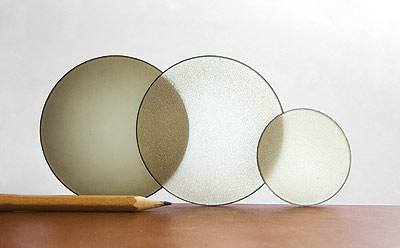
Plates of polycrystalline diamond
|
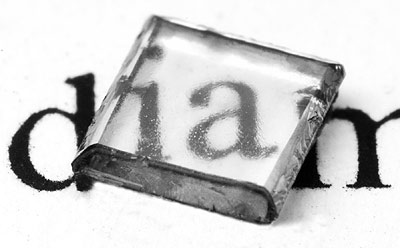
Photo of a 2.5×2.5×0.3 mm
CVD diamond monocrystal
|
For the needs of micro- and nanoelectronics, the technique of epitaxial deposition of monocrystalline CVD diamond on substrates of natural IIa diamond has been developed. The synthesized monocrystalline layers of CVD diamond have orientation (100), the quality exceeding the quality of the substrate, and a thickness of 100—1000 μm. On the basis of the synthesized CVD diamond, semiconducting p-type diamond was produced jointly with the Federal State Unitary Enterprise "Istok". This diamond has a record-breaking hole mobility of 1150 cm2/(V · s), which is the highest value achieved in semiconducting diamond when boron is doped by the ion implant method. The produced near-surface highly-doped layer of the p-type allows one to use it as the contact layer in electronic devices. The technique of producing combined substrates up to 100 mm in diameter, which was developed in close cooperation with the Federal State Unitary Scientific & Manufacturing Enterprise "Istok" ensures simultaneous growing of wide-band diamond structures, which are necessary for further developments of high-power semiconducting microwave devices. The production lines, which are used already in silicon engineering, can be used to develop electronic devices on the basis of such 200—500 μm thick plates.
One of the fields, where new materials are produced with the use of high-frequency and microwave discharge plasma, is production of thin films and massive samples of silicon and germanium, both with the natural isotopic composition, and enriched with one of the isotopes of their gaseous fluorides.
A laboratory prototype of the CVD reactor for high-rate
(5 nm/s) deposition of nano- and microcrystalline films of natural silicon from the plasma of a discharge in silicon tetrafluorine (SIF4), which is maintained by the radiation of a technological 24 GHz gyrotron, has been developed (A. V. Vodopyanov, S. V. Golubev, and P. G. Sennikov). In contrast with conventional chemical technologies, the researchers managed to run the process of decomposition of silicon tetrafluorine and deposition of the produced silicon on a substrate in a plasmochemical reactor in one stage, which allowed them to decrease the content of foreign impurities in the final product significantly. The advantages of the developed technique made it possible to produce films of 28Si with a record-breaking level of isotope purity, specifically, 0.999986 ± 0.000003, i.e. an isotopic dilution of not more than 10 ppm from 28SiF4 with an extremely high enrichment of 0.9999969. Another on-going development is the high-rate technique of deposition of germanium isotopes in the powder form from the microwave discharge plasma, consequent melting them together, and stretching of monocrystals.
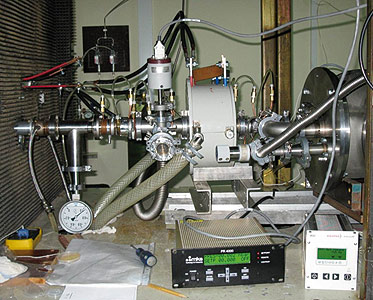 |
Plasmochemical reactors for production of isotope-pure silicon. This reactor allows one to produce silicon samples that have record-breaking isotope purity, specifically,
a 28Si content of 99.9985%. Production rate is 2 g/h |
The recent advance in nuclear physics is notably due to the wide use of ECR sources of multicharge ions. A great contribution to improvement of such sources has been made by IAP researchers A. V. Vodopyanov, S. V. Golubev, V. G. Zorin, and S. V. Razin. The obtained results gave rise to an almost universal transition to the use of the radiation of high-power millimeter-wave gyrotrons in ECR sources. In the recent decade, many unique devices were developed, which made it possible to achieve record-breaking currents (up to 200 mA), basic luminance of the produced ion beams (up to 70 A/(π • mm • mrad)2), and efficiency of using initial gases, which is rather important when working with rare isotopes. Much of the experimental success is closely related to the development of adequate methods for simulation of various ECR discharge regimes in the magnetic trap. Today, scientists are seeking actively the possibility to use the radiation of multicharge ions of stannum, which are produced in an ECR discharge, for the needs of modern nanolithography. In a laboratory experiment, line emission of multi-charge Sn ions with a required wavelength of 13.5 nm was produced in a band with a relative width of 1% at a power level of 50 W. The efficiency of conversion of the microwaves absorbed in the plasma to extreme ultraviolet radiation (about 1%) is comparable with the world-best achievements obtained by using pulsed laser systems.
Due to the fast progress in the telecommunication field, the potentialities of the up-to-date satellite communication systems are limited now by the occurrence of multipactor discharges in them. Therefore, the calculation of electric strength of radio technical vacuum devices is an important step of designing new systems of satellite communication. In the process of studying the multipactor thresholds in satellite communication systems, the IAP team led by V. E. Semenov developed a theoretical model lacking the main drawbacks typical of the approximation of uniform electromagnetic fields, which had been used universally earlier to calculate the electric strength of radio technical vacuum systems. Specifically, abandoning of the uniform-field approximation allowed one to:
- find that a single-sided multipactor discharge can be formed on the output window of high-power microwave devices in the absence of d.c. electric or magnetic fields, as well, which was considered earlier as an absolutely necessary condition of the return of secondary electrons to the emission surface. It is shown that in this case, the discharge formation conditions depend significantly on not only the amplitude of the high-frequency electric field on the window surface, but the amplitude of the magnetic field as well;
- confirm the basic importance of the allowance for the spread of secondary electrons over initial velocities for accurate prediction of multipactor formation in actual systems. Currently, the European State Agency (ESA), which coordinates the development of the EU space program, requires that this effect must be taken into account in all software tools developed for numerical testing of space communication systems;
- develop efficient algorithms of numerical simulation of the multipactor discharge, which are used currently in almost all calculations of the electric strength of space communication systems.
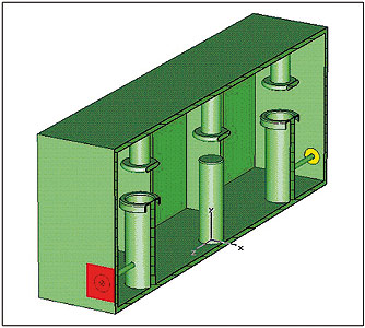
Components of satellite communication systems, which are used to test the results of numerical multipactor simulation in the framework of the European EVEREST project