|
Department of plasma technology physics
РУССКИЙ
Results
1. Monocrystalline diamond deposition at high speed in a CVD reactor with highly focused wave beams in millimeter wavelength range |
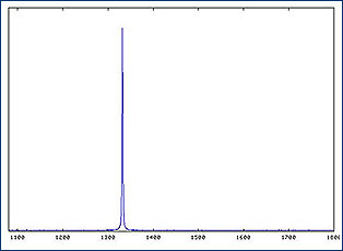
Using two intersecting focused electromagnetic wave beams in millimeter wavelength range in reactor for CVD synthesis of diamond, continuous microwave discharge in a hydrogen-methane mixture with a high power density, of the order of 1000 - 1500 W/cm3, was obtained. It has been demonstrated that in such discharge it is possible to achieve record speeds of homoepitaxial growth of single-crystal diamond up to 120 μm/h in gas mixture without addition of nitrogen (less than 1 ppm). Width of the peak corresponding to diamond in Raman spectrum is 1.65 cm-1, which corresponds to high-quality diamond.
|
|
|
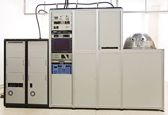
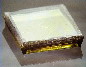
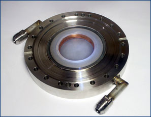
MPA CVD reactor for diamond synthesis
|
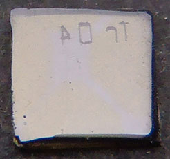
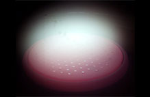
Photo of epitaxial layer of diamond grown at a speed of 120 μm/h
|
| |
|
|
References:
A.L. Vikharev, A.M. Gorbachev, D.B. Radishev, Physics and application of gas discharge in millimeter wave beams, J. Phys. D: Appl. Phys. 52 (2019) 014001 (13pp), https://doi.org/10.1088/1361-6463/aae3a3
A.M. Gorbachev, A.L. Vikharev, M.A. Lobaev, D.B. Radischev, S.A. Bogdanov, V.V. Chernov, А.В. Козлов, Microwave discharges in gases at conditions of the high power densities, Xth International Workshop on Microwave Discharges: Fundamentals and Applications (Zvenigorod, Russia, September 3 – 7, 2018)
|
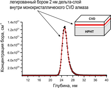
2. 2 nm boron delta-doped layer inside single-crystal CVD diamond |
Technology is developed for production of heavily boron doped layers with thickness 1-2 nm and boron concentration (5-10) 1020 cm-3 during single-crystal CVD diamond growth. Layers demonstrate hole mobility of 100-200 cm2/V s with high surface concentration of carriers concentration (1013 cm-2). Application of technology enables obtaining diamond material with properties suitable for creation of diamond electronics devices. |
|
|
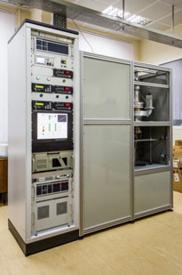
CVD reactor for diamond doping
|
depth profile of boron concentration inside diamond
|
| |
|
|
| 3.Single-crystal CVD diamond films with thickness up to 0.5 mm, grown on HPHT and natural diamond substrates with dimensions from 3.5x3.5 mm to 5x5 mm |
| Development of technology for epitaxial CVD growth of single-crystalline CVD diamond on HPHT and natural diamond substrates with quality exceeding the quality of used substrates. |
|
|
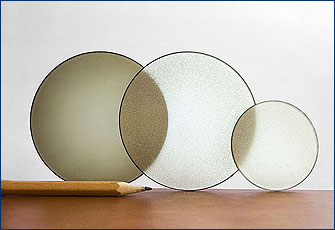
Single-crystal CVD diamond layer of 200 μm thickness grown on HPHT diamond substrate
|
Raman spectrum of single-crystal CVD diamond,
FWHM of diamond peak - 1.8 cm-1
|
|
References:
A. L. Vikharev, A. M. Gorbachev, A. B. Muchnikov and D. B. Radishchev, Study of microwave plasma-assisted chemical vapor deposition of poly-and single-crystalline diamond films, Radiophysics and Quantum Electronics, 50 (2007) № 10-11, 913
A.B.Muchnikov, A.L.Vikharev, A.M.Gorbachev, D.B.Radishev, V.D.Blank, S.A.Terentiev, "Homoepitaxial single crystal diamond growth at different gas pressures and MPACVD reactor configurations", Diamond and Related Materials, 19 (2010) 432
A. A. Altukhov, A. L. Vikharev, A. M. Gorbachev, M. P. Dukhnovsky, V. E. Zemlyakov, K. N. Ziablyuk, A. V. Mitenkin, A. B. Muchnikov, D. B. Radishev, A. K. Ratnikova, Yu. Yu. Fedorov, Characterization of single-crystal diamond grown from the vapor phase on substrates of natural diamond, Semiconductors, March 2011, Volume 45, Issue 3, pp 392-396
Muchnikov A.B., Vikharev A.L., Gorbachev A.M., Radishev D.B., Comparative study of homoepitaxial single crystal diamond growth at continuous and pulsed mode of MPACVD reactor operation, Diamond and Related Materials, 2011, v.20, p.1225-1228.
Ratnikova A.K., Dukhnovsky M.P., Fedorov Yu.Yu., Zemlyakov V.E., Muchnikov A.B., Vikharev A.L., Gorbachev A.M., Radishev D.B., Altukhov A.A., Mitenkin A.V., Homoepitaxial single crystal diamond grown on natural diamond seeds (type IIa) with boron-implanted layer demonstrating the highest mobility of 1150 cm2/Vs at 300K for ion-implanted diamond, Diamond and Related Materials, 2011, v.20, p.1243-1245
|
| 4. Combined single-crystalline and polycrystalline CVD diamond substrate |
| Development of technology for CVD growth of combined single-crystalline and polycrystalline CVD diamond substrates for needs of diamond electronics |
|
|
Microwave discharge under combined mono- and polycrystalline diamond substrate in 2.45 GHz CVD reactor |
Combined single-crystalline and polycrystalline CVD diamond substrate after grafting process, 76mm in diameter |
|
References:
A. L. Vikharev, A. M. Gorbachev, M. P. Dukhnovsky, A. B. Muchnikov, A. K. Ratnikova, and Yu. Yu. Fedorov, Combined Singlecrystalline and Polycrystalline CVD Diamond Substrates for Diamond Electronics, Semiconductors, 2012, Vol. 46, No. 2, pp. 263–266
A.B. Muchnikov, A.L. Vikharev, D.B. Radishev, V.A. Isaev, O.A. Ivanov, A.M. Gorbachev, A wafer of combined single-crystalline and polycrystalline CVD diamond, Materials Letters, 2015, 139, pp.1-3; http://dx.doi.org/10.1016/j.matlet.2014.10.022
|
| 5. Polycrystalline diamond disks of 0.2-1.5 mm thickness and 50-75 mm in diameter |
| Fabrication of polycrystalline diamond disks of 0.2-1.5 mm thickness and 50-75 mm in diameter with high quality (FWHM of diamond peak in Raman spectrum - 2.5-3.5 cm-1, longitudinal heat conductivity – 15-19 W/K•cm) |
|
|
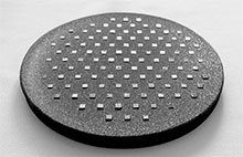
Freestanding polycrystalline CVD diamond samples
|
Polycrystalline CVD diamond samples, polished (d=50mm, h=1.5mm)
and unpolished (d=75mm, h=0.5mm)
|
| |
|
|
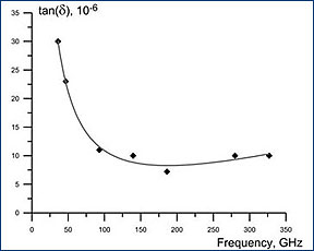
| 6. Gyrotron window with cooling system made from polycrystalline diamond disk |
| Fabrication of exit window of high-power microwave devices (gyrotrons) using polycrystalline diamond disks |
|
|
|
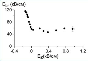
Dependence of tangent of losses in diamond disk on microwave frequency
|
| |
|
|
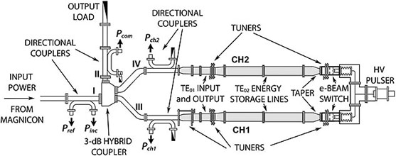
| 7. Two channel active microwave pulse compressors on frequency 11.4 GHz |
|
|
Schematic diagram of the experimental setup for tests of the two-channel microwave pulse compressor with switches employing electron beam triggering
|
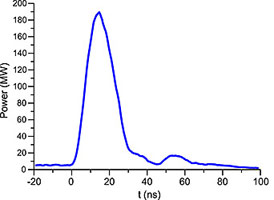
Oscilloscope trace of the compressed pulse
|
| |
|
|
 |
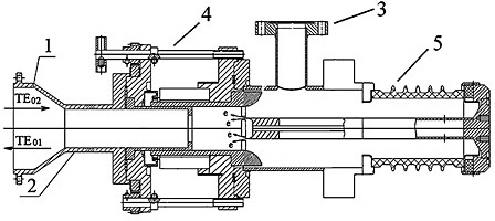 |
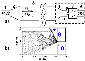
| (a) Schematic diagram of the one channel of the compressor: 1 - input TE01 mode waveguide; 2 - input taper; 3 - storage cavity; 4 - conical taper; 5 - waveguide section; 6 - diaphragm; 7 - TE012-mode switch cavity; 8 - cathode; 9 - anode plate. (b) Instantaneous computed distribution of electrons inside the switch cavity at a beam current of 200 A and cathode voltage of 100 kV |
Scheme of the switch employing electron beam triggering: 1 – taper, 2 - cylindrical waveguide, 3 - pumping port, 4 - external tuning mechanism, 5 - insulator |
|
References:
O.A. Ivanov, V.A. Isaev, M.A. Lobaev, A.L. Vikharev, J.L. Hirshfield, A resonance switch employing an explosive-emission cathode for high-power RF pulse compressors // Appl. Phys. Letters, V.97, pp. 031501-031503, (2010)
O.A. Ivanov, V.A. Isaev, M.A. Lobaev, L. А.L. Vikharev, and J. L. Hirshfield, High power microwave switch employing electron beam triggering with application to active RF pulse compressors // Phys. Rev. ST Accel&Beams, 14, 061301, (2011)
A.L. Vikharev, O.A. Ivanov, A.M. Gorbachev, M.A. Lobaev, V.A. Isaev, S.G. Tantawi, J.R. Lewandowski, J.L. Hirshfield, X-band active SLED-II RF pulse compressor with plasma switches // Phys. Rev. ST Accel.&Beams, 14, 2011
O.A. Ivanov, M.A. Lobaev, А.L. Vikharev, A.M. Gorbachev , V.A. Isaev, J.L. Hirshfield , S.H. Gold A.K. Kinkead, Active Microwave Pulse Compressor Using an Electron-Beam Triggered Switch // Phys. Rev. Letters, 110, 115002, (2013) |
| |
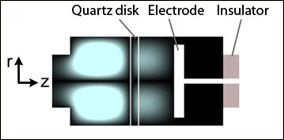
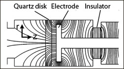
| 8. Investigation of multipactor discharge initiation and suppression on dielectric surfaces |
| Experimental study of a multipactor discharge and its suppression on a dielectrics surface in a microwave cavity |
|
|
|
Instantaneous distribution of microwave field in resonator
|
Distribution of electrostatic field lines inside microwave resonator for quartz disk 6 mm thick
|
Dependence of threshold microwave field of multipactor discharge initiation on amplitude of electrostatic field for quartz
|
| |
|
|
|
References:
O.A. Ivanov, M.A. Lobaev, V.A. Isaev, A.L. Vikharev, Experimental Study of a Multipactor Discharge on a Dielectrics Surface in a High-Q Microwave Cavity, Plasma Physics Reports, 36 (2010) № 4, 336
M.A. Lobaev, O.A. Ivanov, V.A. Isaev, A.L. Vikharev, Effect of Inhomogeneous Microwave Field on the Threshold of Multipactor Discharge on a Dielectric, Technical Physics Letters, 35 (2009) № 12, 1074
Ivanov O.A., Lobaev M.A., Isaev V.A., Vikharev А.L., Suppressing and Initiation of Multipactor Discharge on a Dielectric by an External DC Bias, Phys. Rev. ST AB, 13 (2010) 022004 |
|