РУССКИЙ
The Laboratory of Microwave Discharge Physics was created in 1995 in IAP RAS. In 2009 it was renamed to the Laboratory of Microwave Discharge Physics and Carbon Material Synthesis, in 2014 – reorganized into Department of Plasma Technology Physics, consisting of two laboratories:
Main research interests:
- Physics of freely localized microwave discharge in wave beams
- Microwave plasma assisted chemical vapour deposition of mono and polycrystalline diamond films
- Development of high rate deposition of diamond films in high density plasma, created by microwave radiation in millimeter wave band
- Investigation of physical properties of CVD diamond
- Synthesis of semiconducting CVD diamond
- Development of solid-state electronic, acoustoelectronic and optical devices based on diamond films
- Laser cutting and mechanical processing (lapping and polishing) of diamond materials
- Development of active microwave pulse compressors with distributed plasma switches
- Investigation of conditions of multipactor discharge initiation and suppression on dielectric surfaces
 |
 |
 |
 |
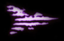
Microwave discharge in two crossed wave beams, frequency 40 GHz
|
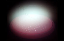
Microwave discharge under combined mono- and polycrystalline diamond substrate in 2.45 GHz CVD reactor
|
Polycrystalline CVD diamond samples, polished (d=50mm, h=1.5mm) and unpolished (d=75mm, h=0.5mm)
|
Monocrystalline CVD diamond layer on HPHT diamond substrate
|
Institute of Applied Physics RAS,
46 Ul'yanov Street , 603950, Nizhny Novgorod , Russia